DivIDE MEMORY


DivIDE interacts with ZX Spectrum using I/O accesses  or automatically by replacing original ZX-ROM with its own memory, when CPU fetch from an entry-point is detected (and such behavior is somehow allowed).

DivIDE contains 8 kB ROM (could be not present, EPROM or EEPROM, in the third case it's in-system reprogrammable) and 32-512 kB RAM. DivIDE can use system from 3rd 8k bank of its RAM, this is suitable especially for safe system development. Accidental EEPROM damage (due to unlucky out from crashed code) is fused by the on-board jumper.

Memory mapping

Memory mapping could be invoked manually (by setting CONMEM), or automatically (CPU has fetched opcode form an entry-point). Automatic mapping is active only if EPROM/EEPROM is present (jumper EPROM is closed) or bit MAPRAM is set. Automatic mapping occurs at the begining of refresh cycle after fetching opcodes (M1 cycle) from 0000h, 0008h, 0038h, 0066h, 04c6h and 0562h. It's also mapped instantly (100ns after /MREQ of that fetch is falling down) after executing opcode from area 3d00..3dffh. Memory is automatically disconnected in refresh cycle of the instruction fetch from so called off-area, which is 1ff8-1fffh.

The one-instruction delay could be used to distinguish between nested calls to the same place. For such trick you will place different instruction at the entrypoint address, than is in original ZX ROM. So the first call wil execute
original instruction, but subsequent one  will jump to another code, because divIDE memory was already mapped, with its changed opcode. It's great for 100% avoidance of nested NMI, which cannot be implemented using pure combinatorial hardware workaround. It allows divIDE to use INT for timing, when divIDE code is performed (external calls will map later divIDE off and continue in #38h original service, but nested INTs can jump to  another work, and mapping off is of course undesirable there).

In automatic mapping, when MAPRAM is set, in location 0000h-1fffh appears write-protected Bank No.3, instead of EEPROM/EPROM. The meaning-priority is (from lowest to highest) EPROM jumper -> MAPRAM -> CONMEM. So because that jumper is no more significant when MAPRAM or even CONMEM is set, it's used to distinguish between fused or unfused EEPROM state for CONMEM mode. 

So, when CONMEM is set, there is:
0000-1fffh - EEPROM/EPROM/NOTHING(if empty socket), and this area is flash-writable if EPROM jumper is open.
2000-3fffh - 8k bank, selected by BANK 0..1 bits, always writable.

When MAPRAM is set, but CONMEM is zero, and entrypoint was reached:
0000-1fffh - Bank No.3, read-only
2000-3fffh - 8k bank, selected by BANK 0..1. If it's different from Bank No.3, it's writable.

When MAPRAM is zero, CONMEM is zero, EPROM jumper is closed and entrypoint was reached:
0000-1fffh - EEPROM/EPROM/NOTHING(if empty socket, so open jumper in this case), read-only.
2000-3fffh - 8k bank, selected by BANK 0..1, always writable.

Otherwise, there's normal speccy memory layout. No modified ROM, no shit.

[*] Change introduced with r'_gal contents (16kB ram paging):
- divIDE behaves as normally,until the condition CONMEM=0,MAPRAM mode on,JP2(E)open and bank1=1 happens
- then, divide RAM maps in immediately as 16kB banks (paired banks 0:1 or 2:3)
  and the CONTROL REGISTER will get new meaning:
  [ RETURN, WRITEENABLE, X, X, X, X, X, BANK0 ]
- setting RETURN serves as exit from this mode
- BANK0 selects one of these two 16k banks
- after initiation, WRITEENABLE depends on latest BANK0 state (0 enables)
- after initiation, the state of RETURN is 0 and the state of BANK0 unknown


DivIDE in standard mode

DivIDE control register (write only) 227 ($E3) in original DivIDE mode:
D7 D6 D5 D4 D3 D2 D1 D0
CONMEM MAPRAM X X X X BANK1 BANK0

This register is write-only (readed data will be unknown). All bits are reset to '0' after each power-on. Unimplemented bits, marked 'X', should be zeroed for future compatibility issues with more than 32kB RAM DivIDEs.

Bits BANK1 and BANK0 select the 8k bank, which normally appears in area 2000-3fffh, when divide memory is mapped.


value 10xxxxBB

Bit CONMEM forces EPROM/EEPROM to 0000-1fffh and by BANK 1..0 selected bank to area 2000-3fffh, regardless to the actual divIDE state or to physical presence of EPROM/EEPROM. Bank in area 2000-3fffh is always writable, and in 0000-1fffh always appears EEPROM/EPROM, which is writable when EPROM jumper is open. Use it in third-party utilities for loading system or modules, or in system's auto-upgrade process.
adress 0 - 8191 ($0000 - $1FFF) adress 8192 - 16383  ($2000 - $3FFF)

8kB EEPROM
( writable only if jumper E is open )

8kB RAM page (selected with bank1+bank0)
( writable ram pages 0 - 3 )


value 01xxxxBB  (with closed jumper E)

Bit MAPRAM can be set to '1' only (when it's '1', only power-on can return it to '0'). This bit allows 8k bank No.3 to act as EPROM/EEPROM, and write-protects it. Set it when system image is loaded into bank No.3 and you want to safe probe it till the next power-on. Set it also when you haven't EPROM/EEPROM, and you want to use system. (Because u will possibly re-install it from MAPRAM mode, you will need CONMEM to override writeprotect. Because after returning to BASIC you rely on original ROM, you must reset automapper, which could be left in undesired state by previous bus transactions. Because it could be done only by fetching code from off-area, u must set DI, then call 1ffbh ('RET'), ten CONMEM, loading image, releasing CONMEM and setting MAPRAM, then EI. Then the return is safe.)
adress 0 - 8191 ($0000 - $1FFF) adress 8192 - 16383  ($2000 - $3FFF)

8kB RAM 3
( write protect - eeprom emulation )

8kB RAM page 0 - 3 (selected with bank1+bank0)
( writable ram pages 0 - 2, page 3 is write protected )


DivIDE with allram mode support (with R"GAL chip)

DivIDE control register (write only) 227 ($E3) before allram activation (original DivIDE mode):
D7 D6 D5 D4 D3 D2 D1 D0
CONMEM MAPRAM X X X X BANK1 BANK0


For allram mode activation you need disconnect CONMEM+active MAPRAM+set BANK1+open jumper JP2(E):

JUMPER setting in allram (for ZX48/128)
JUMPER setting in allram (for +2A / +3)

This all instructions must be writed in assembler with disable IM1 interrupt (ZX rom will disconnect):
1) open jumper JP2(E)
2) OUT 227, 66
- active allram mode (after allram activation will memory layout undefined)
3) use any of next OUT commnads:


Yet is ALLRAM MODE active and DivIDE controll register use new layout :

D7 D6 D5 D4 D3 D2 D1 D0
RETURN
(allram off)
WRITE ENABLE X X X X X BANK0


Allram memory paging

OUT 227, BIN 0000000 = connect read only 16kB ram (8kB pages 0+1)
OUT 227, BIN 0100000 = connect writable 16kB ram   (8kB pages 0+1)

OUT 227, BIN 0000001 = connect read only 16kB ram (8kB pages 2+3)
OUT 227, BIN 0100001 = connect writable 16kB ram   (8kB pages 2+3)

OUT 227, BIN 100000xx = disable allram mode (mapram is active) and connect EEPROM+writable RAM 0 - 3
(after this OUT you can use original controll register layout, but any next OUT 227 with CONMEM=0+BANK1=1 active allram. For 100% return to original DivIDE mode close jumper JP2 (E).

If jumper JP2 (E) is closed, then DivIDE will switched to original mode (with active mapram).


NMI button in allram mode

In allram mode don't work divide automapper, but NMI button will disabled if CPU read instruction opcode from adress 0000h, 0008h, 0038h, 0066h, 04c6h, 0562h and 3D00h-3DFFh. NMI is automatically enabled in refresh cycle of the instruction fetch from so called off-area, which is 1ff8-1fffh. This feature is used in new version of BS-DOS system for DivIDE.


DOWNLOAD new R"GAL chip firmware
 R"GAL - new GAL version with new allram mode support
 R GAL  - original (old) GAL version without allram mode


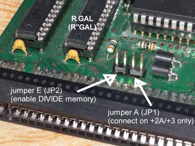
Allram feature is available only on DivIDE interface with new R"GAL chip. DivIDE with this GAL is possible buy at DIVIDE SHOP. Old DivIDE interface can be also upgraded if you replace R-GAL chip with new R"GAL (possible buy in same shop)